TM 55-4920-402-13&P
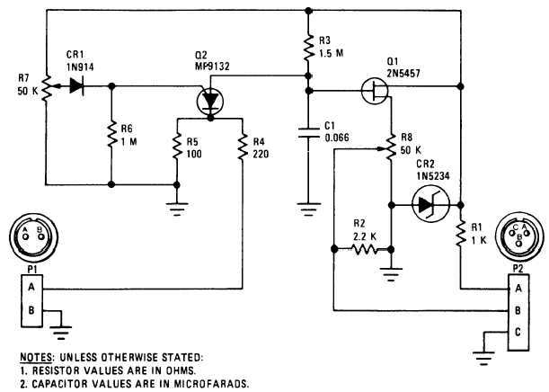
Figure 4-16. Signal simulator B4305, Schematic Diagram
4-19. Signal Simulator Tests. These tests will
determine operational capability of the signal
simulator.
a. Refer to figure 4-17 for schematic diagram
and Table 4-15 for resistance checks as
necessary.
b. Perform Signal simulator check below:
(19 Connect DC Power Supply (+) Positive
lead to connector P2 pin A, and (–) Negative
lead to connector P2 pin C.
(2) Connect oscilloscope leads from channel
A input to connector Pin B, and channel B input
to connector P1 pin A.
(3) Adjust power supply for + 9VDC.
Observe that channel A wave form is an ex-
ponential sawtooth with a period of 110 mS, ±
5% with an amplitude of 90 mV peak-to-peak ±
5%.
(4) Channel B wave from shall be a short
pulse occuring at the negative stage of channel A
sawtooth, with an amplitude of 2.5V ± 10%.
Add: Entire page as shown on draft. Third
sentence in first note should read: “Do not ex-
ceed 40 watts. ”
Change 4
4-15

